Methodologie for Hardware Retro Engineering
Static Analysis
OSINT
First step is to look for open source documentation regarding the device
- Manufacturer website
- teardowns (check on IFixIT website)

- If device is FCC (Federal Communications Commission, USA) certified, there is an alphanumerical code physically present on the device.
This code can be used on FCC Website for documentation or Dominic Spill website
The idea is to get pictures of the insight of the device to ease futur teardown and user guide / technical datasheet.
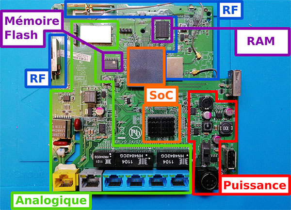
Macroscopic analysis
Once the device is teared down, we frequently face PCB (Printed Circuit Board) and peripherals.
The idea is to identify those such as :
- PSU
- Sensors
- Standard
- Interfaces
- Screens
- Buttons
- Microphones S
- peakers
- ...
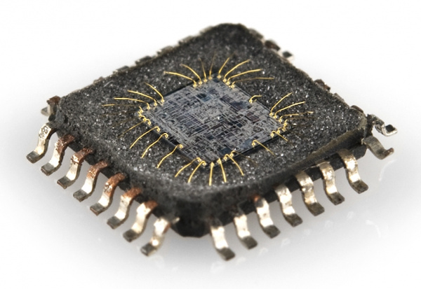
Surface-mount technology
It’s good to know what’s behind :
- TO220
- SOT23
- QFP
- TSOP
- BGA
- ...

For the elements directly soldered on the board (SMD) here are some useful websites


Otherwise datasheets can be found by searching chips references online.
If there is only a foundry logo, it can be searcher up in the bellow database and then search up on their websites.

If there are no documentations one of the solutions might be to check what’s the chip doing by looking at their in & out pins using oscilocops and look with other chips that would do similar things on manufacturers catalogues.
Another solution would be to unsolder the chip and place it on another PCB or a breadboard for in deep analysis using one of the following solutions :
- DIP (Dual In-line Package).
- ZIF (Zero Insertion Force).
- Or try to auto detect the chip using an universal programmer like TNM5000.
Doing so might require dedicated PCB or direct soldering on the chips. Here are some refs :
 https://blog.quarkslab.com/flash-dumping-part-i.html
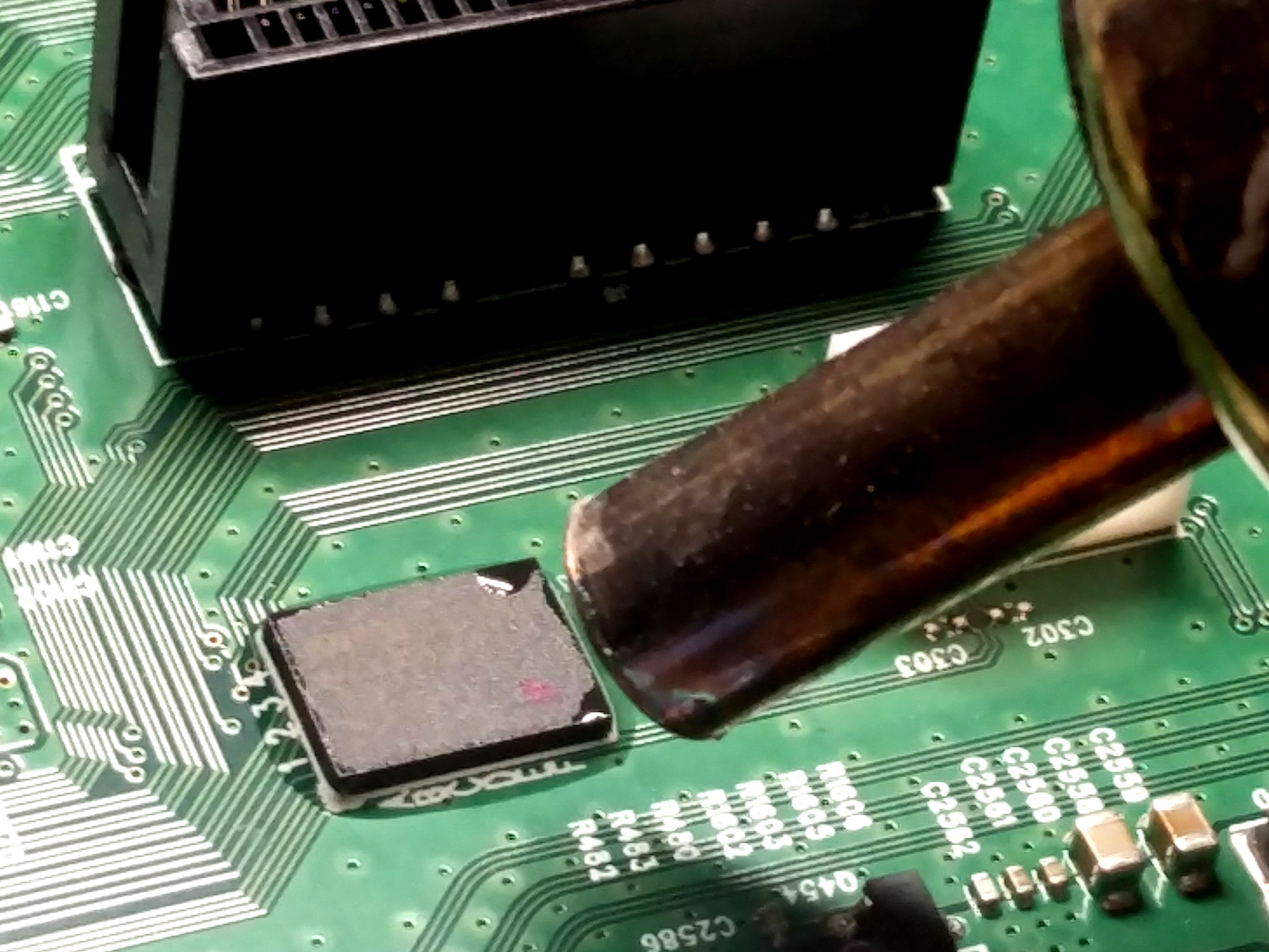 https://blog.quarkslab.com/flash-dumping-part-ii.html
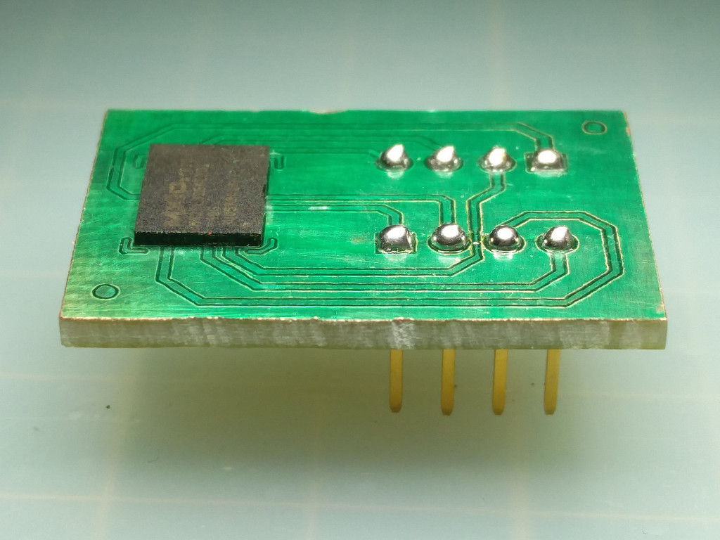
PCB Lines analysis
This is useful to determine the lines of test points, or dedicated and isolated test points. These points might lead to USART (universal synchronous and asynchronous receiver-transmitter), a JTAG port (oint Test Action Group) or any other proprietary test ports.
It might be needed to partialy or fully reverse the PCB to have a better understanding of how each elements are linked together and how they interact with each others. This might be done using a multimeter that will make some noise when both sides of a link are tested simultaniously. (it might be useful to have test needles to be more precises).
If there are multiple lines of copper, or components that aren’t easily accessible, it will require more invasive techniques such as desoldering chips (which might be reversible but complicated to achive) or even desolder the entire board to see each elements if we have a spare unit to sacrifice.
The Art of PCB Reverse Engineering from Ng Keng Tiong is a good extension for more informations
For hardware reverse at an industrial level, these documents might be useful :
PCB-RE: Tools & Techniques from Ng Keng Tiong
Dynamic Analysis
Once the Static Analysis is done, we have a better view of the components that populate the board, the links in between them, as well as test points.
These informations are useful to be used as attack surface
Communication interfaces
The communication between components is generally made using standardised interfaces. These informations are really useful to understand what is going on on the board
To identify Which type of communication is used, we’ll use a logical analyser. This tool once connected on the test points will record the tensions level on the links several millions of times per seconds in order to make a chronogramme of the logical states
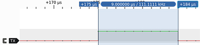
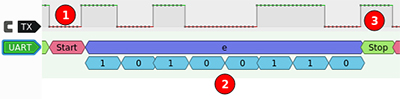
USART (Universal synchronous and asynchronous receiver-transmitter)
USART is used to assure simultaneous communication between two chips
Here are some elements that need to be known to use USART :
<baudrate> <bits per symbole><parity><stop bit>
The most used configuration is the following :
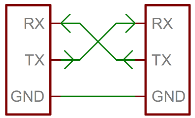
115200 8NUSART is an RX pin for Reception and TX pin for Transmission. These pins have to be swapped in between the two chips
SPI (Serial Peripheral Interface)
SPI allow communication between a chip and other components like sensors or actuators.
To do so, it requieres 3 lines MOSI, MISO, CLK as well as a selction line CS per device as shown on the side schematic
These configuration might be used for small flash memory storage
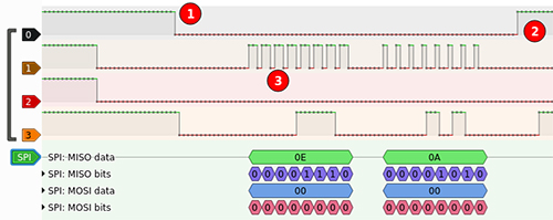
The CLK line is on (dot3). It tells the Slave there is data available for them (line 1)
At the same time the slave reply the byte to the Master (line 3)
The CS line tells that Slave that the operation start (dot1) and stop (dot2) (line 0)
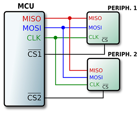
- SCLK: Serial Clock (output from master)
- MOSI: Master Out Slave In (data output from master)
- MISO: Master In Slave Out (data output from slave)
- CS: Chip/Slave Select (often active low output from master to indicate that data is being sent)
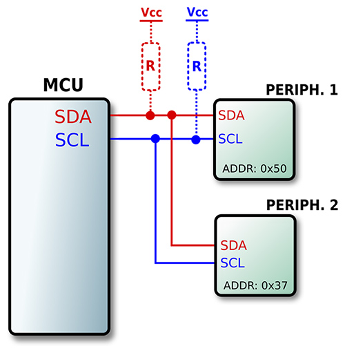
I²C (Inter-Integrated Circuit)
I²C is a bit different from SPI, I²C is linking multiple peripherals to a controler using the same links
This means that only one peripheral can speak at a defined time. each ones have a dedicated address to identify them
It use 2 lines SDA (for data) and SCL (for clock).
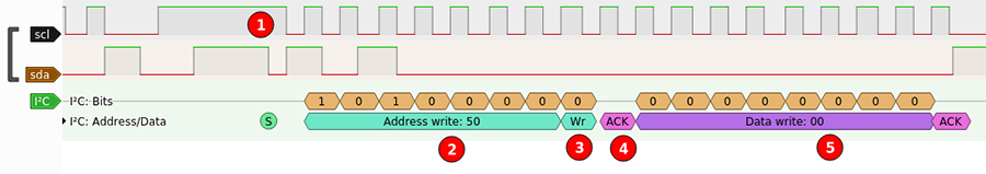
Dot1 : the MCU start the communication
Dot2 : The MCU send the address with which they want to communicat
Dot3 : The type of opération (0 = Write, 1 = Read)
Dot4 : The peripheral acknoledge the request
Dot5 : The controler send the data to the peripheral and then the peripheral acknoledge that the data is written
Communication decoding
USART, SPI and I²C allow to exchange informations across multiple devices. however, the data format in it might varie depending the manufacturer or field of application.
Reading the data that goes through the link isn’t that complexe but being able to translate it to actual instruction might need so time reading specific documentation for products.
Memory extraction
The most valuable targets are the ones that store data or source code in non volatile memory. Here is a list of the various elements that containe data or source code :
- EEPROM
- Flash (some kind of evolved EEPROM)
- MCU (microcontrolers (that have embeded storage or are linked to an EEPROM)
For small memories that communicate with the MCU can be dumped using a raspberry pi and flashrom (it might require desoldering the chip or solder on it directly)
Depending on the MCU, and the PCB configuration, it is also possible to use some universal programmers using test points or directly by plugging it over the chip to acces debug interfaces (JTAG, SWD, ISP, PDI, UPDI, etc)
some MCU will be read protected. however it might be possible in some case to bypass this protection using fault injection for exemple
It’s important at this point to read detailed documentation to know what can be achieved and how
Firmware Reverse Engineering
 https://cutter.re/